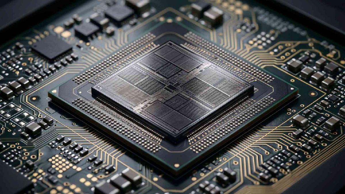
The race to develop next-generation DRAM memory chips is heating up, with industry giants Samsung and SK hynix adopting distinct strategies to meet the burgeoning demands of AI-driven data centers. As first reported by Wccftech, both companies are navigating a tight memory market, grappling with the challenges posed by increased demand for high-bandwidth memory (HBM), DRAM, and other essential chips.
Samsung is reportedly exploring the use of gate-all-around FET (GAAFET) fabrication technology for its upcoming DRAM offerings. This shift in approach could signify a move towards leveraging techniques historically associated with NAND flash manufacturing. GAAFET technology allows for a more efficient control of current flow in transistors, potentially leading to enhanced performance and lower power consumption in DRAM chips. Such advancements will be crucial as the memory landscape evolves, especially under the pressures of AI workloads that require higher speeds and capacity.
On the other hand, SK hynix is concentrating on a vertical stacking approach, which involves layering memory chips to increase density and reduce footprint. This strategy could offer significant advantages in terms of performance and efficiency, particularly as the demand for faster, more efficient memory solutions continues to rise. By stacking chips vertically, SK hynix aims to improve data transfer rates and reduce latency, which are critical factors in AI applications.
The backdrop of this competition is a memory market experiencing unprecedented strain due to the rapid expansion of AI technologies. The integration of AI into a wide array of computing applications has led to a surge in demand for memory products, which are essential for managing the vast amounts of data processed in AI operations. The simultaneous push for HBM, DRAM, and other memory types has created a challenging environment for manufacturers, who must secure raw materials and optimize production techniques to keep pace.
Both Samsung and SK hynix are positioning themselves to capitalize on this market demand, but their chosen paths reflect different aspects of innovation in memory technology. Samsung’s GAAFET approach could represent a significant leap in manufacturing capabilities, potentially setting new standards for performance in DRAM. Meanwhile, SK hynix’s vertical stacking method could redefine how memory is utilized in data center configurations, offering a compact solution that meets the requirements of modern AI applications.
As these two tech behemoths advance their respective strategies, the implications for the broader memory market will be profound. Increased competition is likely to drive innovation, resulting in faster, more efficient memory chips that can handle the complex needs of AI and other demanding applications. This evolution is not only critical for the companies involved but also for the technology landscape as a whole, influencing everything from gaming to enterprise solutions.
In summary, the contrasting approaches of Samsung and SK hynix in the pursuit of next-generation DRAM technology highlight the complex interplay between innovation and demand in the memory semiconductor industry. The outcomes of these strategies will be closely watched as the industry adapts to the relentless pace of AI advancement.
Samsung is a global leader in semiconductor technology, known for its advancements in memory chips and displays. SK hynix is another prominent player, recognized for its high-performance DRAM and NAND flash memory products, and both companies are crucial to the future of computing technology.
Image credit: Wccftech
This article was generated with AI assistance and reviewed for accuracy.