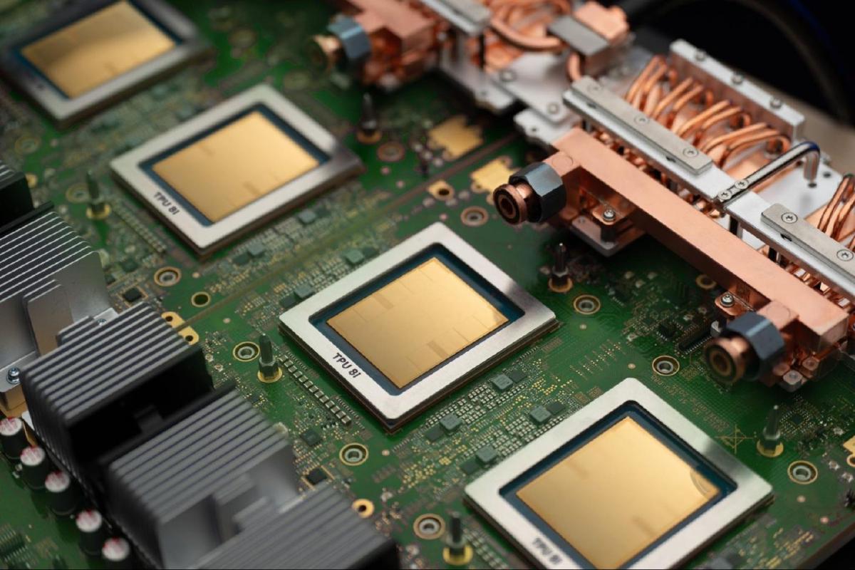
As the race to advance artificial intelligence continues, Google is taking significant steps to enhance its custom chip offerings. The company is reportedly launching its new ‘Frozen V2’ Tensor Processing Units (TPUs), which are set to optimize performance for its Gemini models. This new design eliminates the reliance on TSMC’s chip-on-wafer-on-substrate (CoWoS) packaging technology, according to a report by Morgan Stanley, as first reported by Wccftech.
Google’s decision to hardwire SRAM directly onto the silicon of its TPUs marks a strategic shift that could have a profound impact on the efficiency of its AI computing capabilities. By integrating Static Random-Access Memory (SRAM) into the chip itself, Google aims to reduce power consumption and production costs, making its offerings more competitive against NVIDIA’s high-priced and often scarce GPUs.
The company’s latest TPU design reflects a broader trend in the tech industry, wherein major players are striving to develop chips that can meet the escalating demands of AI workloads while bypassing the limitations associated with traditional manufacturing techniques. The use of TSMC’s CoWoS technology, while beneficial in certain contexts, can introduce complexities and delays in production, which Google seems keen to eliminate.
Google’s move comes at a time when the demand for AI processing power is skyrocketing. Organizations are increasingly leveraging AI for a myriad of applications, from natural language processing to advanced data analytics. As such, having a robust and cost-effective chip designed specifically for these tasks is crucial for staying ahead in the competitive landscape.
By streamlining the design of its TPUs, Google not only enhances their performance but also positions itself as a formidable contender in the AI chip market. The integration of SRAM into the silicon structure allows for faster data access and processing speeds, essential for the performance-intensive applications that Gemini aims to support.
The implications of this development extend beyond just Google. Other tech giants like Amazon are also investing heavily in custom chip designs, including their Trainium processors, which focus on reducing costs and power usage in AI workloads. As these companies vie for dominance in the AI sector, innovations like Google’s Frozen V2 TPUs will likely set the standard for future advancements.
The Gemini project has been a focal point for Google, aiming to enhance its AI capabilities across various platforms. By aligning its TPU technology with this initiative, Google is signaling its commitment to delivering high-performance, cost-effective solutions to meet the growing needs of AI developers and enterprises.
In summary, Google’s introduction of the Frozen V2 TPU represents a significant technical advancement that could reshape its approach to AI computing. By eliminating TSMC’s CoWoS packaging and integrating SRAM directly onto the silicon, Google is setting a new standard for performance and efficiency in the rapidly evolving landscape of artificial intelligence.
Google, founded in 1998, has become synonymous with search and cloud computing. In recent years, it has expanded its focus towards artificial intelligence and machine learning, making significant investments in hardware development to support these initiatives.
Image credit: Wccftech
This article was generated with AI assistance and reviewed for accuracy.