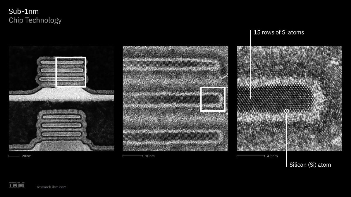
Elon Musk has raised concerns regarding IBM’s recent announcement of its 0.7-nanometer chip manufacturing technology, labeling the terminology they used as misleading. During the presentation, IBM touted its new process as the most advanced available, but Musk contends that the nomenclature does not accurately reflect the actual dimensions of the transistors produced using this technology.
As reported by Wccftech, Musk emphasizes that the naming convention should be based on the number of atoms rather than the arbitrary numerical designations currently in use. His criticism comes at a time when the semiconductor industry is under intense scrutiny for its marketing practices, especially as companies strive to showcase advancements in manufacturing capabilities.
Musk’s remarks are especially significant given his involvement in the Terafab project, which aims to produce an impressive one terawatt of computing capacity each year. This ambitious initiative reflects Musk’s commitment to pushing the boundaries of technology and data processing. His strong stance on how chip manufacturing technologies should be labeled indicates a desire for greater transparency in an industry where precise specifications can have a substantial impact on performance metrics.
The nomenclature used in semiconductor manufacturing has been a topic of debate for years. Traditionally, companies have assigned process node names based on the smallest features produced, which has led to confusion as the naming conventions have not kept pace with actual manufacturing capabilities. Musk argues that a terminology based on the physical characteristics of the components, such as the number of atoms involved, would provide a clearer understanding of the technology’s capabilities.
IBM’s recent announcement was intended to showcase advancements in their chip design, which aim to enhance performance while reducing power consumption. The company has committed to pushing the envelope in semiconductor technology, but Musk’s commentary suggests that more clarity is needed in how such advancements are communicated to both consumers and industry stakeholders.
While Musk’s critique may provoke discussions within the semiconductor community, it also highlights a fundamental tension between technical precision and marketing strategies. As the race for smaller, more efficient chips continues, the industry may need to reevaluate its naming conventions to ensure that they reflect the true nature of the technology.
Musk’s focus on transparency and precision resonates with ongoing concerns about the direction of chip manufacturing and its implications for industries reliant on high-performance computing, such as gaming and artificial intelligence. With the Terafab project poised to impact how computing power is generated, Musk’s insights into naming conventions could lead to broader changes in industry standards.
As chip manufacturers like IBM continue to push for innovation, Musk’s perspective adds an interesting layer to the discussion about how advancements are marketed. Whether or not this leads to a shift in industry nomenclature remains to be seen, but it underscores the need for clear communication in a field where technical details are paramount.
IBM, a longstanding leader in the semiconductor market, has introduced various technologies over the years to maintain its competitive edge, but Musk’s viewpoints may inspire a reevaluation of how these advancements are presented. As the industry evolves, clear and accurate terminology will be essential in helping consumers and professionals alike navigate the complex landscape of chip technology.
Image credit: Wccftech
This article was generated with AI assistance and reviewed for accuracy.